DC2611A-A
Demonstration Board, LTC6955IUKG, Clock Fanout Buffer, Clock & Timing

Reikia daugiau?
| Kiekis | |
|---|---|
| 1+ | 563,830 € |
Informacija apie produktą
Produktų apžvalga
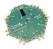
DC2611A-A demonstration circuit features the LTC®6955 ultralow jitter 11 output fanout buffer. By default, the DC2611A-A is powered from a single 3.3V supply. An option is provided to power to the DC2611A-A from dual supplies, allowing for the LTC6955’s output supply pins to connect to an LTC Silent Switcher® and the LTC6955 input supply pin to connect to a low noise LDO. The differential inputs and six of the differential outputs are populated with 0.5" spaced SMA connectors. These outputs are AC-coupled with 50 ohm transmission lines making them suitable to drive 50 ohm impedance instruments. The remaining four differential outputs are terminated with 100 ohm. A calibration path is provided to aid in accurate LTC6955 propagation delay measurements. The calibration path can be also reconfigured as a DC path, which allows for a convenient method of locking the LTC6955 outputs to an external PLL/VCO.
- Easy to set up to evaluate the performance of the LTC6955IUKG
- SE, IN–, <5GHz termination
Techniniai duomenys
Analog Devices
Clock & Timing
Demo Board LTC6955IUKG
No SVHC (21-Jan-2025)
LTC6955IUKG
Clock Fanout Buffer
-
Techniniai duomenys (1)
Teisinė ir aplinkosaugos informacija
Šalis, kurioje paskutinį kartą gamintojo atliktas stambus gamybos procesasKilmės šalis:Philippines
Šalis, kurioje paskutinį kartą gamintojo atliktas stambus gamybos procesas
„RoHS“
Gaminio atitikties sertifikatas